
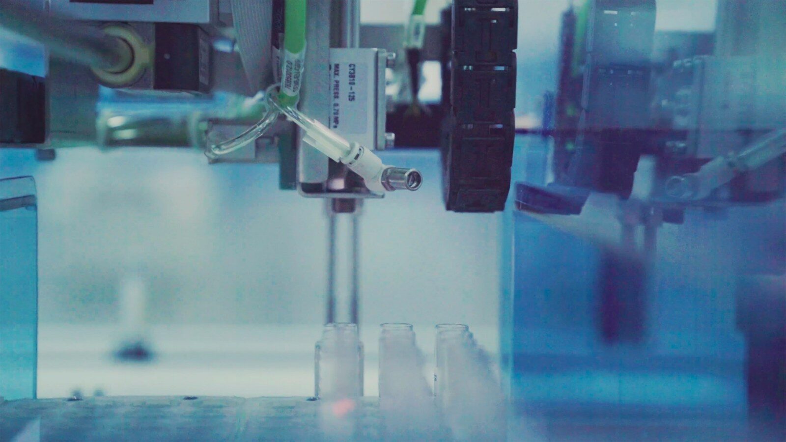
A robotic laboratory system guided by machine learning has mapped a materials-manufacturing problem while physically testing fewer than one per cent of roughly 5,000 possible experimental combinations. The US Department of Energy says the AutoBot platform could shorten the slow trial-and-error stage of developing advanced materials.
The demonstration focused on metal-halide perovskites, a family of materials studied for solar cells, detectors and other light-sensitive electronics. AutoBot selected experiments involving temperature, timing and humidity, then used the results to decide which test would be most informative next.
What did the robot discover?
The system identified humidity as the strongest factor affecting material quality. Follow-up experiments supported the prediction and indicated that moderate or low humidity could help the material form a favourable crystal structure during its early stages.
The headline efficiency does not mean the robot fabricated every possible material or proved that one recipe is ready for a commercial solar panel. It means a closed-loop system used a small set of strategically chosen experiments to predict relationships across a much larger design space.
Why is closed-loop experimentation important?
Materials research often involves changing several variables at once. Testing every combination can consume months of laboratory time and large quantities of chemicals. In a closed loop, software proposes an experiment, robotics carries it out, measurements are returned to the model and the next experiment is selected using what has been learned.
This approach can make scientists more productive while preserving the need for human judgement. Researchers still define the goal, choose safe operating limits, validate unexpected results and decide whether a material has practical value.
Could AutoBot be used beyond solar materials?
The team says the method can be adapted to plastic-like semiconductors and oxide materials. Potential applications include electronics, detectors and improved energy technologies. Each material system will require new equipment, measurements and validation.
The research used the Molecular Foundry at Lawrence Berkeley National Laboratory and was supported by the Department of Energy, the National Science Foundation and partner institutions. Its immediate contribution is a demonstrated research workflow; wider industrial impact will depend on replication and scale-up.
Source: US Department of Energy research highlight, 10 November 2026.
Image: Testalize.me via Unsplash.